





The €400 Million Question
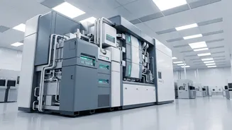
In the hyper-competitive world of semiconductor manufacturing, staying ahead means making colossal bets. The latest and most significant is the adoption of ASML’s new High-NA EUV lithography machines. Priced at approximately $380 million to $400 million each,
these systems are more than double the cost of their predecessors. They are the size of a double-decker bus, require hundreds of engineers months to assemble, and represent the absolute cutting edge of manufacturing technology. The Dutch firm ASML is the only company in the world capable of producing these marvels of engineering, giving it a unique and powerful position in the global tech supply chain. The investment is staggering, but for giants like Intel, TSMC, and Samsung, the cost of falling behind is even greater.
What is High-NA EUV and Why Does It Matter?
At its core, chipmaking is a process of printing incredibly complex circuit patterns onto silicon wafers. For years, this has been done using a technology called Extreme Ultraviolet (EUV) lithography. Think of it as the world’s most precise projector. However, as the industry pushes towards ever-smaller transistors—a trend described by Moore’s Law—the current generation of EUV tools is hitting its physical limits. This is where High-NA (High Numerical Aperture) EUV comes in. By using a completely redesigned system of larger, more complex mirrors, these new machines can focus light with unprecedented precision. The result is the ability to print circuit lines just 8 nanometers wide, a significant improvement over the 13nm resolution of previous machines. This leap allows chipmakers to pack nearly three times as many transistors into the same area, leading to chips that are significantly more powerful and energy-efficient. Crucially, it simplifies the manufacturing process by reducing the need for complex and costly multi-patterning techniques.
The Race Among the Giants
The world's three dominant chipmakers have distinct strategies for this new era. Intel has been the most aggressive, becoming the first company to assemble a commercial High-NA EUV machine at its Oregon R&D facility and recently announcing it is using the technology in high-volume manufacturing for its Core Ultra Series 3 processors. This 'first-mover' advantage is a bold gamble to reclaim its leadership in process technology. Meanwhile, Samsung and TSMC, the world's two largest contract chip manufacturers, have also committed to the technology. Samsung plans to introduce High-NA EUV for producing its advanced DRAM memory chips by 2028. TSMC, known for its more cautious and deliberate approach, is targeting 2030 for its deployment in advanced logic chips. Their recent commitments signal an industry-wide consensus that High-NA is not just an option, but a necessity for producing the chips that will power the AI revolution.
Beyond the Machine: A New Ecosystem
The shift to High-NA is not as simple as just buying a new machine. It requires a fundamental change in the surrounding ecosystem. In a rare show of unity, rivals Intel, TSMC, and Samsung are now collaborating with ASML on an initiative to develop larger photomasks—the 'stencils' used to project circuit designs. The plan is to move from the current 6-inch standard to a new 12-inch format. This change is crucial because the new High-NA optics expose a smaller area at a time. Larger masks will allow bigger chips to be printed in a single pass, increasing manufacturing productivity by an estimated 40% and making the enormous cost of the machines more justifiable. This industry-wide effort shows that the challenges are too large for any single company to solve alone.
What This Means for You
While the details are highly technical, the outcome of this multi-billion dollar race will directly impact consumers. The transition to High-NA EUV is the foundational step needed to manufacture the sub-2-nanometer chips of the near future. These are the processors that will enable breakthroughs in artificial intelligence, power more sophisticated and efficient smartphones, and drive the next wave of high-performance computing. The immense investment in these €400 million machines is a direct bet on a future where our devices are smarter, faster, and more integrated into our lives than ever before. It's a complex, expensive, and crucial change that begins with a single, incredibly precise beam of light.