









A New Frontier in AI Hardware
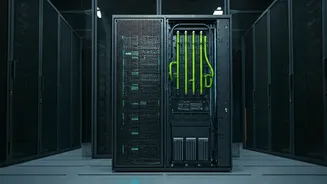
Imagine a supercomputer condensed into a single server cabinet. That's the promise of Kyber, a next-generation AI architecture designed to power the most demanding artificial intelligence models. The system achieves this by integrating 144 of the most powerful
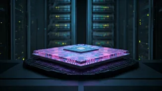
graphics processing units (GPUs) into a single, cohesive unit, allowing them to function as one colossal computer. This approach, known as advanced packaging or multi-chip integration, is seen as the future of semiconductor design. Instead of building one enormous, complex chip—which is expensive and prone to defects—designers use a collection of smaller, specialised chips, or 'chiplets'. These are then interconnected on a sophisticated base, or substrate, to work in harmony. This method boosts performance, improves energy efficiency, and can even lower costs by making manufacturing yields higher for smaller components.
The 'Orthogonal Backplane' Breakthrough
The secret sauce in Kyber's design is a highly complex piece of hardware called an 'orthogonal backplane', which is a type of printed circuit board (PCB). This component allows the compute trays holding the GPUs to be mounted vertically, connecting directly to a rear switch tray. This clever design eliminates the messy and inefficient 'cable jungle' traditionally needed to link so many processors, drastically reducing the distance signals have to travel and cutting down on communication delays (latency). The result is a system with unprecedented density and computational power, essential for training the massive AI models that are reshaping industries from medicine to finance. It represents a significant leap in solving the engineering challenges of scaling up AI infrastructure.
Innovation Hits a Manufacturing Wall
Despite the brilliant design, a major hurdle has emerged on the factory floor. The very component at the heart of the innovation—the advanced PCB midplane—is proving exceptionally difficult to manufacture reliably. Reports from the semiconductor research firm SemiAnalysis indicate that these production challenges are forcing a significant delay, pushing the product's launch back by over a year, potentially into 2028. This kind of delay is not uncommon in the semiconductor industry, where bleeding-edge designs often push the limits of current manufacturing capabilities. The board in question is reportedly a 78-layer hybrid material marvel that is incredibly complex to produce without defects. Issues with manufacturing yield—the percentage of usable products from a production run—can quickly derail timelines and budgets, as even small defects can render the entire expensive component useless.
Market Impact and a Window for Competitors
A delay of this magnitude does more than just push back a product launch; it opens a window of opportunity for competitors. Major rivals in the AI chip space now have an extended period to advance their own high-density solutions and potentially capture market share that Kyber was poised to dominate. Cloud service providers and large-scale data center operators, who are the primary customers for these systems, may now look to alternative solutions to meet their scaling needs. NVIDIA, the company behind the Kyber architecture, has reportedly also had to cancel a backup plan and scale back the specifications of the eventual product, further complicating its roadmap. The situation underscores a critical lesson in the tech industry: a groundbreaking design is only as good as your ability to manufacture it at scale. For now, the celebration of Kyber's engineering feat is on hold as the company grapples with the immense challenge of turning its vision into a physical reality.