






The Tandem Cell Revolution
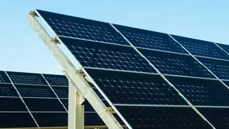
For years, the solar industry has relied on single-junction silicon cells, which are nearing their theoretical efficiency limit of around 29%. While commercial panels have become much cheaper, their efficiency has been plateauing in the low-to-mid 20%
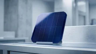
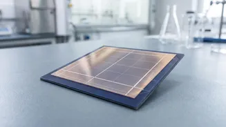
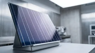
range. Enter the tandem solar cell, a technology that pairs a traditional silicon cell with a layer of a crystal material called perovskite. This 'solar panel sandwich' approach is revolutionary because the two materials capture different parts of the light spectrum. The perovskite layer absorbs high-energy blue light, while the silicon layer below captures lower-energy red light. Together, they convert more of the sun's energy into electricity than either could alone, with a theoretical maximum efficiency of over 40%.
Breaking the 30% Barrier
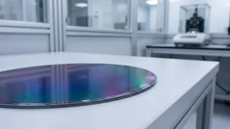
The 30% efficiency mark has long been seen as a crucial psychological and commercial barrier. Recently, solar technology leader LONGi announced it had achieved a record 30.1% efficiency for a perovskite-silicon tandem cell built on a commercial-grade M6 wafer. This was certified by Germany's prestigious Fraunhofer Institute for Solar Energy (Fraunhofer ISE). This is a significant leap, not just from a scientific perspective, but because it was achieved on a commercial-size wafer, not just a tiny lab-scale sample. It signals that the technology is moving from pure research toward industrial viability. This achievement required overcoming key manufacturing challenges, such as preparing large-area perovskite films and developing new metallization processes.
Why Wafer Size Matters
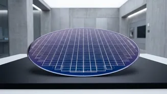
In modern solar manufacturing, size is a critical factor in cost. The industry has been moving towards larger silicon wafers, primarily the M10 (182mm) and G12 (210mm) formats. Larger wafers allow manufacturers to produce higher-power modules, which can reduce costs throughout the value chain. A panel with more power means fewer panels are needed for a project of a given size. This translates into lower balance-of-system (BOS) costs, which include things like mounting hardware, wiring, inverters, and labour. For large utility-scale solar farms, these savings can be substantial. The debate between M10 and G12 often comes down to a trade-off between manufacturing efficiency and logistical handling.
Efficiency Changes the Entire Equation
This is where the 30% efficiency milestone becomes a game-changer for large wafers. With standard silicon cells, the economic benefit of moving to ever-larger wafer sizes has limits. But when you combine a massive leap in efficiency with a large-format wafer, the benefits multiply. A G12 wafer featuring a 30% efficient tandem cell can produce significantly more power than one with a 23% efficient conventional cell. This dramatically improves the cost-per-watt metric, which is the holy grail of the solar industry. The higher the efficiency, the more electricity is generated from the same physical area, making every other associated cost—from land and installation to maintenance—more economical. The new efficiency record strengthens the argument that investing in production lines for larger, more powerful tandem-cell modules is the most logical path forward.
The Road to Commercialisation
Despite this breakthrough, several hurdles remain before these super-efficient panels are widely available. The primary challenge is long-term durability. Perovskite materials can be sensitive to moisture, heat, and UV exposure, and they must be proven to last for 25 to 30 years in real-world conditions to be commercially viable. Scaling up production from a single record-setting cell to millions of modules without losing efficiency or consistency is another major challenge that companies are now tackling. However, the industry is confident. With major players like LONGi investing heavily in mass production research, the transition from lab records to rooftop reality is accelerating.