









The Unsung Hero of AI Power
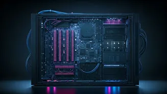
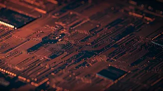
Beneath the headlines about teraflops and large language models lies a less glamorous but critical component: the substrate and packaging. Think of an AI chip as a megastar performer. The circuit board and its advanced packaging are the stage, wiring,
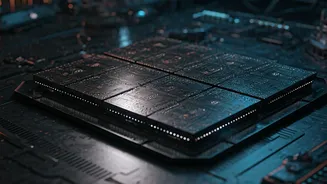
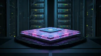
and support structure that make the performance possible. This isn't your standard green motherboard. For AI accelerators like NVIDIA's Blackwell series, it involves a sophisticated process called Chip-on-Wafer-on-Substrate (CoWoS). This technique allows multiple high-performance silicon dies and stacks of high-bandwidth memory (HBM) to be integrated into a single, massive package. This integration is the secret sauce to the incredible performance of modern GPUs, but it's also the source of a growing headache.
A Crisis of Complexity and Physics
The sheer ambition of NVIDIA's designs is running into fundamental physics. As chips like the GB200 and the upcoming Rubin integrate more processing units and memory, the packages become larger and more complex. A significant issue is "substrate warpage." The package is a sandwich of different materials—silicon for the chips, organic materials for the substrate—that all expand and contract at different rates when heated during manufacturing. This mismatch can cause the entire package to physically bend or warp, leading to connection failures and catastrophically low production yields. This problem becomes exponentially worse as the package size increases. In fact, these manufacturing execution concerns recently forced NVIDIA to scrap an ambitious four-chip design for its future Rubin Ultra GPU, reverting to a more manageable two-chip version.
The Supply Chain Bottleneck
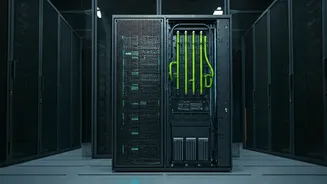
This complexity creates a massive bottleneck in the supply chain, which is struggling to keep up. TSMC, the foundry that manufactures these components, has seen its advanced packaging capacity completely booked out years in advance, with NVIDIA reportedly reserving over half of the available supply. Reports from early 2026 show that the production of the Blackwell family of chips has faced significant issues reaching high-volume production, impacting targets and extending the lifespan of older Hopper chips to fill the gap. The challenges aren't just in the chip package itself. Delays have also been reported for specialized Printed Circuit Board (PCB) midplanes, essential components for linking GPUs together in massive rack systems like the Kyber NVL144. Even liquid cooling systems, necessary to manage the immense heat from these systems, have presented overheating and leakage problems, adding to delays.
The High Stakes Race for Solutions
NVIDIA and the entire industry are in a high-stakes race to solve these physical limitations. The demand for advanced packaging is growing at an incredible rate, creating severe shortages. The solution isn't just about building more factories; it requires fundamental innovation. The industry is exploring new materials like glass substrates, which offer better stability than organic ones, and new manufacturing methods like "panel-level packaging." This would move from round silicon wafers to large rectangular panels, allowing more chips to be produced at once with less waste. NVIDIA is reportedly securing exclusive access to these next-generation technologies to maintain its edge. At the same time, the shortages are creating an opportunity for competitors like Samsung and Intel, who are positioning their own packaging technologies as viable alternatives for companies struggling to secure capacity from TSMC.