


What is the story about?
What's Happening?
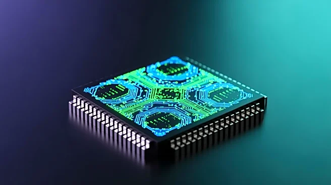
Fudan University has announced the development of the world's first two-dimensional-silicon-based hybrid architecture chip, marking a significant advancement in semiconductor technology. The research, published in the journal Nature, integrates ultrafast flash memory with the mature CMOS process, addressing key challenges in two-dimensional information device engineering. The chip boasts a high yield rate of 94.34% and supports advanced operations, potentially outperforming current Flash memory technologies. This development follows the team's earlier breakthrough with the 'PoX' picosecond flash memory device, which achieved unprecedented storage speeds. The team plans to further integrate this technology into the semiconductor industry, aiming for large-scale application within the next few years.
Why It's Important?
This breakthrough by Fudan University could significantly impact the semiconductor industry by introducing a new standard for memory devices. The integration of two-dimensional materials with CMOS technology promises faster and more energy-efficient data processing, which is crucial for fields like artificial intelligence and big data. The potential to disrupt traditional memory systems and replace hierarchical storage architectures with general-purpose memory could lead to more efficient computing solutions. This advancement may also accelerate the adoption of two-dimensional electronic devices in practical applications, offering a competitive edge in technology development.
What's Next?
The research team plans to establish an experimental base and collaborate with institutions to further develop this technology. They aim to integrate the project to a megascale level within 3 to 5 years, potentially licensing intellectual property to cooperative enterprises. This could lead to widespread adoption of two-dimensional flash memory as a standard storage solution in the AI era. The team's efforts to integrate these devices into existing CMOS production lines may compress the timeline for technological advancements, paving the way for disruptive applications in the future.
Beyond the Headlines
The integration of two-dimensional materials with CMOS technology presents challenges, such as maintaining material integrity on complex substrates. The team's innovative approach to modular integration and high-density interconnection technology addresses these issues, ensuring compatibility with existing platforms. This development highlights the potential for two-dimensional materials to drive fundamental innovations in device mechanisms, offering new possibilities for the semiconductor industry.