


What is the story about?
What's Happening?
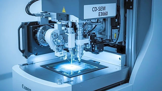
Advantest Corporation has announced the release of its new CD-SEM E3660, designed for the dimensional metrology of photomasks and EUV masks in semiconductor manufacturing. The E3660 offers a 20% improvement in CD reproducibility compared to its predecessor, the E3650, and is aimed at supporting mask manufacturing at the 2nm node and beyond. This development is part of Advantest's strategy to provide comprehensive test solutions across the semiconductor value chain, addressing the increasing complexity and scaling in device fabrication. The E3660 is expected to be deployed in Merchant and Captive Mask Shops, serving as a core tool for advanced mask development and production qualification.
Why It's Important?
The introduction of the E3660 is significant for the semiconductor industry as it addresses the growing need for precise metrology in mask manufacturing, which is crucial for the production of advanced semiconductor devices. As the industry moves towards more complex and curvilinear mask patterns, the E3660's enhanced capabilities will help manufacturers maintain design fidelity and improve throughput. This advancement supports the industry's transition to High Numerical Aperture EUV lithography, expected to be widely adopted by 2027, and reinforces Advantest's position as a leader in semiconductor test equipment.
What's Next?
Advantest plans to target the E3660 for deployment in both Merchant and Captive Mask Shops, which are key facilities for mask production. The company will continue collaborating with research hubs like imec to validate and improve metrology techniques for curvilinear geometries. This ongoing development is expected to enhance the E3660's capabilities further, supporting the industry's shift towards more complex semiconductor designs and manufacturing processes.