






What's Happening?
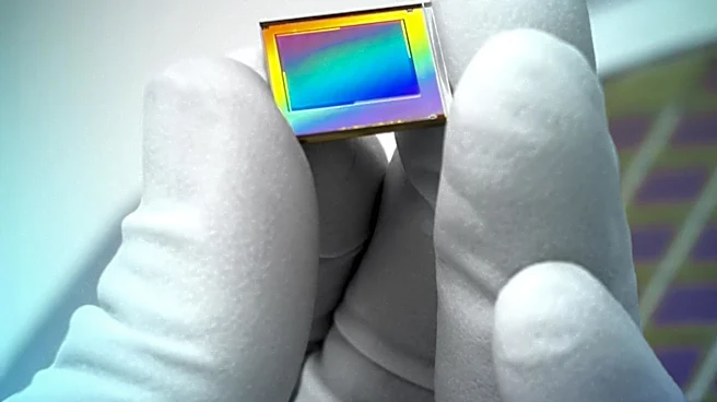
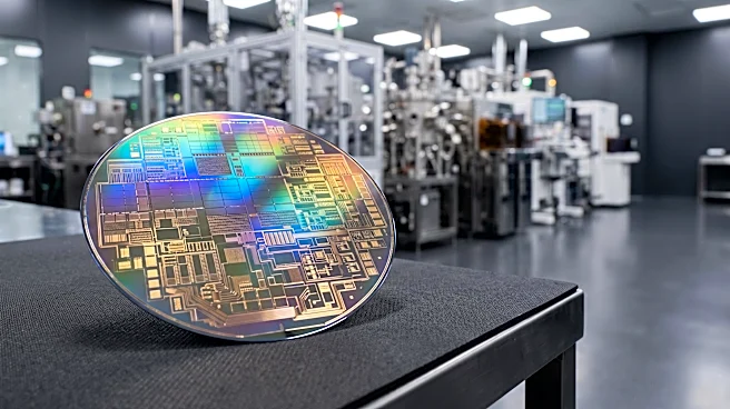
Semiconductor cryogenic cooling involves using extremely low temperatures, ranging from 77 Kelvin with liquid nitrogen to below 10 millikelvin in dilution refrigerators, to alter the behavior of integrated circuits. This process is primarily applied in specialized
research and engineering, rather than in ordinary consumer computers. Cooling a chip to such low temperatures can significantly change carrier mobility, electrical resistance, timing, and packaging characteristics. While lower temperatures can reduce thermal energy and increase carrier mobility, they can also lead to issues like charge 'freeze-out,' altered threshold voltage, and new timing or reliability problems. The design and testing of consumer chips are optimized for standard operating temperature ranges, and attempting to cool them outside these conditions can result in condensation, cracking, unstable operation, or permanent damage. The process of cryogenic testing is highly controlled, involving vacuum chambers, radiation shields, and precise temperature monitoring with Cernox sensors, to ensure stable operation at target temperatures.
Why It's Important?
The distinction between specialized cryogenic cooling and consumer device operation is crucial for understanding technological limitations and advancements. While cryogenic cooling offers significant benefits for research, such as enabling faster transistor operation or reducing electrical loss in specific materials, these advantages do not translate to everyday electronics. The specialized nature of this technology means that the average consumer will not experience its direct benefits in their personal devices. Instead, its importance lies in pushing the boundaries of scientific research, particularly in fields like quantum computing and advanced materials science, where extreme conditions are necessary to observe novel phenomena or achieve specific performance metrics. This research can indirectly lead to future innovations that might eventually trickle down into more conventional applications, but the immediate impact is confined to highly specialized engineering and scientific domains. Misunderstanding this distinction can lead to unrealistic expectations about consumer technology performance and potential damage to devices if improper cooling methods are attempted.
What's Next?
Future developments in semiconductor cryogenic cooling will likely continue to focus on specialized applications, particularly in quantum computing and advanced scientific instrumentation. Research will aim to further refine techniques for achieving and maintaining ultra-low temperatures, exploring new materials and architectures that can leverage these extreme conditions. Efforts may also concentrate on making cryogenic systems more efficient and scalable for industrial research and development. For consumer electronics, the focus will remain on optimizing performance within standard operating temperatures, potentially through advancements in conventional cooling technologies or more energy-efficient chip designs. The insights gained from cryogenic research could inform the development of new materials or design principles that enhance chip performance and reliability, even at ambient temperatures, but a direct application of cryogenic cooling to consumer devices is not anticipated due to the inherent complexities and risks involved.
Beyond the Headlines
The exploration of semiconductor cryogenic cooling highlights a broader theme in technology: the pursuit of extreme conditions to unlock new physical phenomena and engineering capabilities. This field underscores the intricate relationship between temperature, material science, and electrical engineering. It also brings to light the ethical considerations of pushing technological boundaries, particularly regarding the environmental impact of energy-intensive cooling methods and the responsible application of advanced research. The knowledge gained from understanding how integrated circuits behave at near-absolute zero temperatures could lead to breakthroughs in fundamental physics, potentially influencing future generations of computing paradigms beyond current silicon-based limitations. This specialized area of research also emphasizes the importance of interdisciplinary collaboration, combining expertise from physics, materials science, and electrical engineering to tackle complex challenges at the forefront of technological innovation.