


What is the story about?
What's Happening?
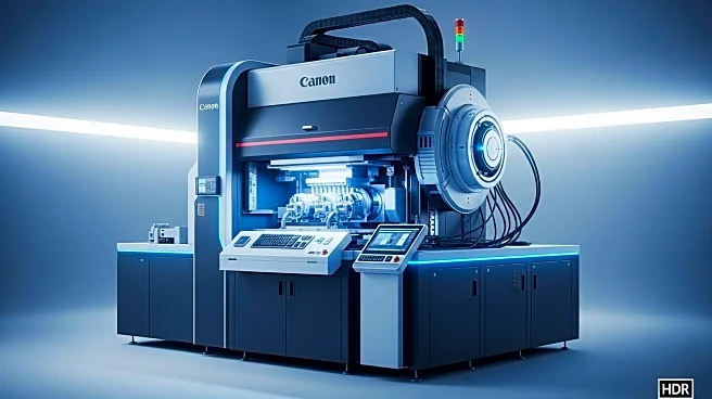
SK Hynix has successfully installed ASML's High-NA EUV lithography system at its M16 fab in South Korea, marking a significant milestone in semiconductor manufacturing. This tool, the first of its kind for mass production, allows for smaller features and higher density DRAM, giving SK Hynix a competitive edge over rivals like Samsung and Micron. The system enhances SK Hynix's ability to develop next-generation DRAM and strengthens its position in the AI-memory market. The High-NA EUV system offers a 40% higher numerical aperture than previous models, enabling features that are 1.7 times smaller and a 2.9 times higher transistor density.
Why It's Important?
The installation of the High-NA EUV lithography tool positions SK Hynix as a leader in advanced semiconductor manufacturing, potentially reshaping the competitive landscape. This technological advancement is crucial for the development of next-generation memory products, which are essential for AI and other high-performance computing applications. By being the first to implement this tool for mass production, SK Hynix gains a strategic advantage, potentially increasing its market share and influencing industry standards.
What's Next?
SK Hynix plans to use the High-NA EUV system to prototype new DRAM structures and simplify existing processes, enhancing cost competitiveness. The company aims to lead the transition to High-NA EUV in DRAM production, expected around the 2030s. This move could drive innovation and set new benchmarks in the semiconductor industry, with potential implications for global supply chains and technology development.