
What's Happening?
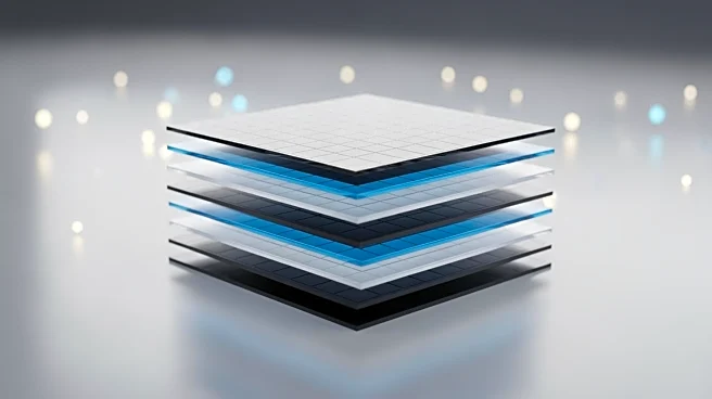
Researchers at King Abdullah University of Science and Technology (KAUST) have set a new record in microchip design by achieving the first six-stack hybrid CMOS (complementary metal-oxide semiconductor)
for large-area electronics. This breakthrough marks a significant advancement in integration density and efficiency, offering new possibilities for electronic miniaturization and performance. The KAUST process involved fabrication steps that did not exceed 150 degrees Celsius, with most steps completed at nearly room temperature, preventing damage to the bottom layers of the chip. The research team, led by Associate Professor Xiaohang Li, focused on refining multiple steps in the fabrication process to enable vertical stacking of transistors, which is seen as a promising solution to the limitations of current design approaches.
Why It's Important?
This development is crucial for the semiconductor industry, which has historically focused on reducing the size of transistors to increase integration density. As the industry approaches quantum mechanical limits and rising costs, the ability to stack transistors vertically offers a new pathway for advancement. Hybrid CMOS microchips, which hold greater promise for large-area electronics compared to conventional silicon chips, are essential for applications in flexible electronics, smart health, and the Internet of Things. The KAUST breakthrough could lead to more efficient and powerful microchips, impacting a wide range of electronic devices and systems.
What's Next?
The KAUST team's achievement sets a new benchmark for future research and development in microchip design. As the industry seeks to overcome the limitations of planar scaling, the focus may shift towards further refining vertical stacking techniques and exploring new materials and processes. This could lead to collaborations between academic institutions and industry players to accelerate the adoption of hybrid CMOS technologies in commercial applications. The implications for consumer electronics, healthcare devices, and IoT systems are significant, potentially driving innovation and growth in these sectors.
Beyond the Headlines
The ethical and environmental implications of this advancement should be considered, as the semiconductor industry faces challenges related to resource consumption and waste management. The KAUST process, which operates at lower temperatures, may offer a more sustainable approach to microchip fabrication. Additionally, the increased efficiency and performance of hybrid CMOS microchips could lead to reduced energy consumption in electronic devices, contributing to broader efforts to minimize the environmental impact of technology.