
What's Happening?
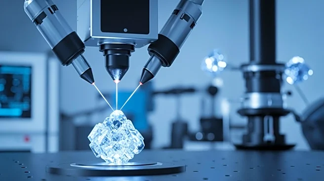
A team led by Elad Harel at Michigan State University has developed a novel method for growing crystals on-demand using lasers and gold nanoparticles. This technique allows for precise 'drawing' of crystals within
a solution of lead halide perovskite, potentially revolutionizing the production of materials used in electronics, such as semiconductors and LEDs. The process involves using a laser to heat a gold nanoparticle, which then triggers crystal formation, allowing for precise placement and control over the crystal's growth.
Why It's Important?
This innovation could significantly impact the U.S. electronics industry by reducing costs and improving the performance of devices that rely on crystalline materials. The ability to precisely control crystal growth could lead to more efficient manufacturing processes and higher-quality products. This method also offers potential environmental benefits by minimizing waste and reducing the need for traditional, less efficient crystal growth techniques.
What's Next?
The research team plans to expand their experiments to include other types of crystals and explore the technique's applicability to a broader range of materials. If successful, this could lead to widespread adoption in the electronics industry, potentially influencing the design and production of future electronic devices. Further testing in real-world applications will be crucial to validate the technique's effectiveness and scalability.
Beyond the Headlines
The development of this laser-based crystal growth technique highlights the intersection of nanotechnology and materials science, showcasing how advancements in one field can drive innovation in another. This approach could pave the way for new research into the properties of materials at the nanoscale, potentially leading to breakthroughs in other areas such as energy storage and biomedical devices.