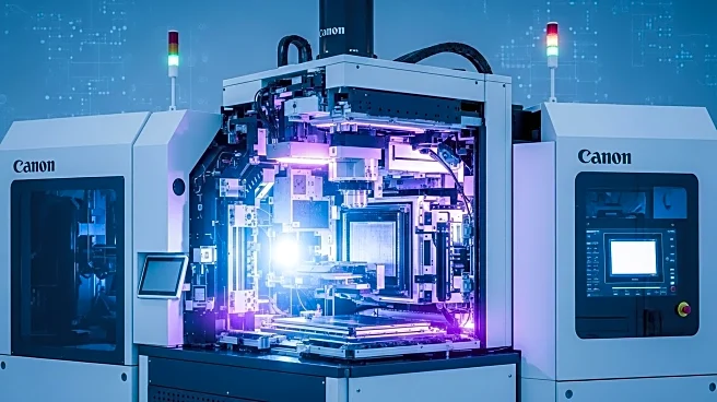

What's Happening?
SK Hynix has successfully installed the first High-NA EUV lithography tool for mass production at its M16 fab in Icheon, South Korea. This tool, developed by ASML, represents a significant advancement in semiconductor manufacturing, allowing for the production of smaller and denser DRAM features. The High-NA EUV system offers a 40% higher numerical aperture compared to its predecessors, enabling features that are 1.7 times smaller and a 2.9 times increase in transistor density. This development positions SK Hynix ahead of competitors like Samsung and Micron in the next-generation memory market. The company plans to use this technology to prototype new DRAM structures and simplify existing processes to enhance cost competitiveness.
Why It's Important?
The installation of the High-NA EUV lithography tool is a critical step for SK Hynix in maintaining its competitive edge in the semiconductor industry. This technology not only enhances the company's ability to produce advanced DRAM but also strengthens its position in the global market against rivals. The advancement is particularly significant as the demand for high-performance memory solutions continues to grow, driven by applications in AI, data centers, and consumer electronics. By adopting this cutting-edge technology, SK Hynix is poised to meet future demands and secure its role as a leader in memory production.
What's Next?
SK Hynix plans to rapidly prototype new DRAM structures using the High-NA EUV system, focusing on features like capacitor trenches and bitlines. The company aims to transition future DRAMs to High-NA EUV technology by the 2030s, reducing risks associated with this shift. As the technology matures, SK Hynix will likely continue to refine its processes to improve efficiency and cost-effectiveness, potentially influencing industry standards and practices.