
What's Happening?
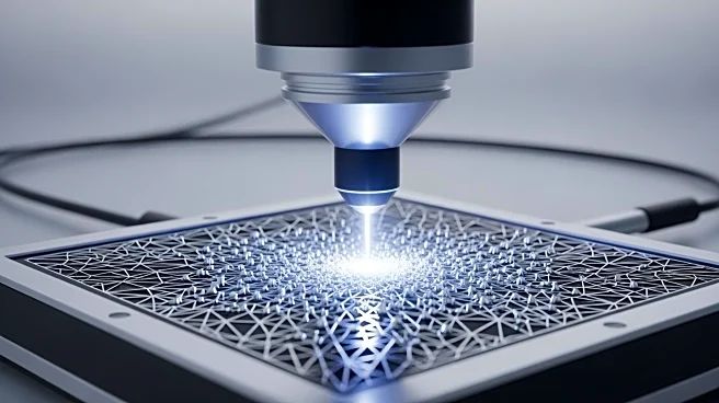
Researchers at Michigan State University have developed a novel method to 'draw' with crystals using laser technology. This technique involves melting gold nanoparticles with a coherent radiation beam
and transferring them to a desired location, where they crystallize instantly upon cooling. The process is conducted in a reaction chamber filled with a lead halide perovskite precursor solution, allowing for precise crystal formation on a glass substrate. This method could revolutionize the production of thin crystal layers used in modern electronics, including space technology, by offering a more accurate alternative to traditional crystallization methods.
Why It's Important?
The ability to precisely control crystal formation has significant implications for the electronics industry, particularly in the production of semiconductors and solar panels. This laser-based technique could lead to the development of ultra-precise circuits, enhancing the performance and efficiency of electronic devices. By improving the accuracy of crystal layer production, this method could reduce manufacturing costs and increase the reliability of electronic components, benefiting industries reliant on advanced electronics.
What's Next?
While the practical application of this crystal drawing technique is still in its early stages, further research and development could lead to its integration into commercial manufacturing processes. The potential for creating ultra-precise circuits suggests that this method could be used in the production of next-generation microelectronics. Continued experimentation and refinement of the technique will be necessary to fully realize its capabilities and integrate it into existing manufacturing frameworks.