
What's Happening?
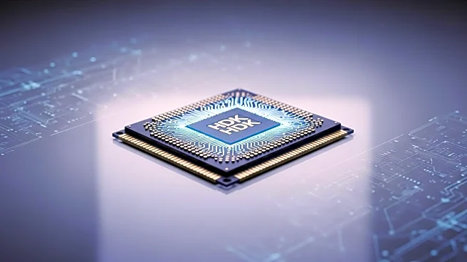
Fudan University has developed the world's first two-dimensional-silicon-based hybrid architecture chip, with research results published in Nature. This chip integrates two-dimensional ultrafast flash memory with the mature CMOS process, overcoming engineering challenges in two-dimensional information devices. The chip supports 8-bit instruction operations, 32-bit high-speed parallel operations, and random addressing, with a yield rate of 94.34%. The research team, led by Liu Chunsen and Zhou Peng, aims to disrupt traditional memory systems and provide faster, lower-energy data support for fields like AI and big data.
Why It's Important?
This breakthrough in memory chip technology could significantly impact the semiconductor industry by offering a new standard for storage solutions. The integration of two-dimensional materials with CMOS processes may lead to advancements in computing power and efficiency, benefiting industries reliant on high-speed data processing. The development could also influence future research and development efforts in memory technology, potentially leading to new applications and innovations.
What's Next?
The research team plans to establish an experimental base and collaborate with institutions to further develop the technology. They aim to integrate the project to the megascale level within 3-5 years, potentially leading to industrial applications. The team will focus on licensing intellectual property rights to cooperative enterprises, accelerating the technology's adoption in the industry.
Beyond the Headlines
The development of this innovative memory chip may prompt discussions about the ethical and legal implications of integrating advanced technologies into existing systems. The potential for disruptive applications could lead to shifts in industry standards and regulatory considerations.