


What is the story about?
What's Happening?
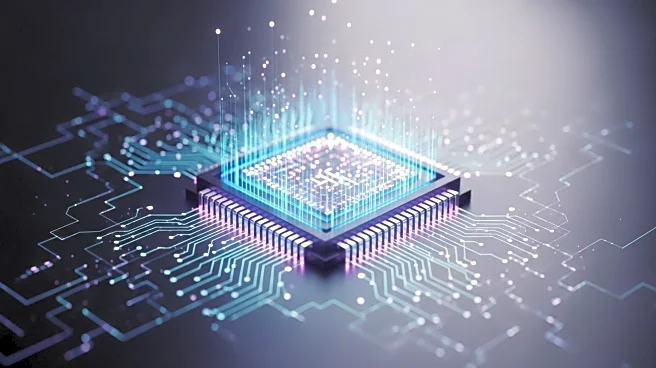
A team of researchers at MIT has made an accidental discovery that could significantly enhance the performance of computer chips. Initially, the team was focused on improving the safety and durability of nuclear reactors by studying material corrosion and cracking. During their experiments, they used a powerful, focused X-ray beam to simulate the intense radiation inside a nuclear reactor. While working with nickel, a common alloy in advanced nuclear reactors, they found that the X-ray beam could precisely 'tune' the strain in the material's crystal structure. This discovery introduces a novel strain engineering technique that could be applied in semiconductor manufacturing to improve optical and electrical performance. The research, published in the journal Scripta Materialia, also achieved its original goal by developing a method for real-time 3D monitoring of material failure in a simulated nuclear reactor environment.
Why It's Important?
The discovery has the potential to revolutionize the semiconductor industry by providing a new method for strain engineering, which is crucial for enhancing the performance of microelectronics. This technique allows engineers to use X-rays to adjust the strain in materials during manufacturing, potentially leading to more efficient and powerful computer chips. The implications for the tech industry are significant, as improved microelectronics can lead to faster and more reliable smartphones, computers, and other devices. This advancement could also drive innovation in various sectors reliant on high-performance computing, including artificial intelligence, data processing, and telecommunications.
What's Next?
The next steps involve further research and development to integrate this technique into semiconductor manufacturing processes. Engineers and companies in the microelectronics sector may explore collaborations with MIT to leverage this discovery for commercial applications. Additionally, the research team may continue to refine the technique and explore its applications beyond microelectronics, potentially impacting other fields such as materials science and nuclear engineering. Stakeholders in the tech industry will likely monitor these developments closely, considering the potential for significant advancements in device performance.
Beyond the Headlines
This discovery highlights the importance of interdisciplinary research and the potential for unexpected breakthroughs in science and technology. The ability to precisely control material properties using X-rays could lead to new innovations in various fields, including energy, healthcare, and environmental science. Ethical considerations may arise regarding the use of advanced technologies in manufacturing and their impact on the environment and society. Long-term, this technique could contribute to more sustainable and efficient production processes, aligning with global efforts to reduce environmental impact.