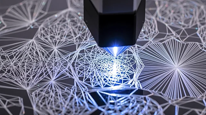

What's Happening?
Researchers at Michigan State University have developed a novel method for drawing crystals using laser technology. This technique involves melting gold nanoparticles with a coherent radiation beam and
transferring them to a desired location, allowing for precise crystallization. The process, which mimics methods used in solar panel creation, could revolutionize the production of thin crystal layers used in modern electronics, offering greater accuracy and efficiency compared to traditional methods.
Why It's Important?
The ability to draw crystals with precision has significant implications for the electronics industry, particularly in the production of microelectronics and space technology. This method could lead to advancements in the creation of ultra-precise circuits, enhancing the performance and reliability of electronic devices. It represents a potential shift in manufacturing processes, reducing waste and improving the scalability of crystal production.
What's Next?
While practical applications of this technique are still in development, researchers anticipate its use in creating advanced microelectronics and potentially influencing the design of future electronic devices. Continued research and experimentation will focus on refining the process and exploring its applications in various industries.
Beyond the Headlines
This development highlights the intersection of materials science and technology, showcasing the potential for innovative approaches to traditional manufacturing challenges. It underscores the importance of interdisciplinary research in driving technological advancements.